 | –≠–ª–µ–∫—Ç—Ä–æ–Ω–Ω—ã–π –∫–æ–º–ø–æ–Ω–µ–Ω—Ç: HCC4013BF | –°–∫–∞—á–∞—Ç—å:  PDF PDF  ZIP ZIP |
HCC/HCF4013B
DUAL 'D' ≠ TYPE FLIP≠FLOP
DESCRIPTION
.
SET-RESET CAPABILITY
.
STATIC FLIP-FLOP OPERATION - RETAINS
STATE INDEFINITELY WITH CLOCK LEVEL
EITHER "HIGH" OR "LOW"
.
MEDIUM-SPEED OPERATION - 16MHz (typ.)
CLOCK TOGGLE RATE AT 10V
.
QUIESCENT CURRENT SPECIFIED TO 20V
FOR HCC DEVICE
.
STANDARDIZED
SYMMETRICAL
OUTPUT
CHARACTERISTICS
.
5V, 10V, AND 15V PARAMETRIC RATINGS
.
INPUT CURRENT OF 100nA AT 18V AND 25
∞
C
FOR HCC DEVICE
.
100% TESTED FOR QUIESCENT CURRENT
.
MEETS ALL REQUIREMENTS OF JEDEC TEN-
TATIVE STANDARD No. 13A, "STANDARD
SPECIFICATIONS FOR DESCRIPTION OF "B"
SERIES CMOS DEVICES"
June 1989
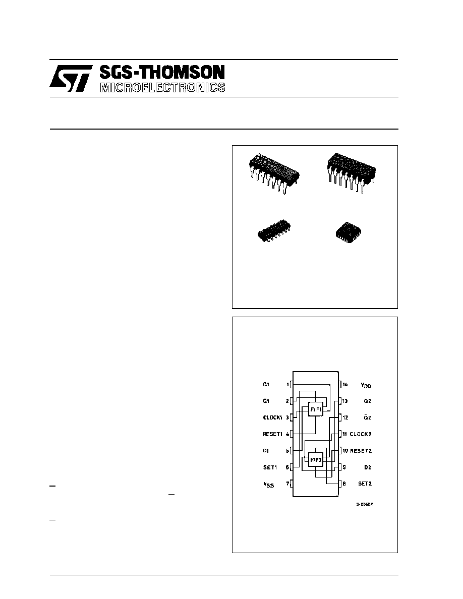
The HCC4013B (extended temperature range) and
HCF4013B (intermediate temperature range) are
monolithic integrated circuits, available in 14-lead
dual in-line plastic or ceramic package and plastic
micropackage.
The HCC/HCF4013B consists of two identical, inde-
pendent data-type flip-flops. Each flip-flop has inde-
pendent data, set, reset, and clock inputs and Q and
Q outputs. These devices can be used for shift reg-
ister applications, and, by connecting Q output to the
data input, for counter and toggle applications. The
logic level present at the D input is transferred to the
Q output during the positive-going transition of the
clock pulse. Setting or resetting is independent of
the clock and is accomplished by a high level on the
set or reset line, respectively.
EY
(Plastic Package)
F
(Ceramic Frit Seal Package)
C1
(Plastic Chip Carrier)
ORDER CODES :
HCC4013BF
HCF4013BM1
HCF4013BEY
HCF4013BC1
PIN CONNECTIONS
M1
(Micro Package)
1/11
ABSOLUTE MAXIMUM RATINGS
Symbol
Parameter
Value
Unit
V
DD
*
Supply Voltage : HCC Types
HC F Types
≠ 0.5 to + 20
≠ 0.5 to + 18
V
V
V
i
Input Voltage
≠ 0.5 to V
DD
+ 0.5
V
I
I
DC Input Current (any one input)
±
10
mA
P
t o t
Total Power Dissipation (per package)
Dissipation per Output Transistor
for T
o p
= Full Package-temperature Range
200
100
mW
mW
T
o p
Operating Temperature : HCC Types
H CF Types
≠ 55 to + 125
≠ 40 to + 85
∞
C
∞
C
T
s t g
Storasge Temperature
≠ 65 to + 150
∞
C
RECOMMENDED OPERATING CONDITIONS
Symbol
Parameter
Value
Unit
V
DD
Supply Voltage : HCC Types
HC F Types
3 to 18
3 to 15
V
V
V
I
Input Voltage
0 to V
DD
V
T
o p
Operating Temperature : HCC Types
H CF Types
≠ 55 to + 125
≠ 40 to + 85
∞
C
∞
C
Stresses above those listed under "Absolute Maximum Ratings" may cause permanent damage to the device. This is a stress rating
only and functional operation of the device at these or any other conditions above those indicated in the operational sections of this
specification is not implied. Exposure to absolute maximum rating conditions for external periods may affect device reliability.
* All voltages are with respect to V
SS
(GND).
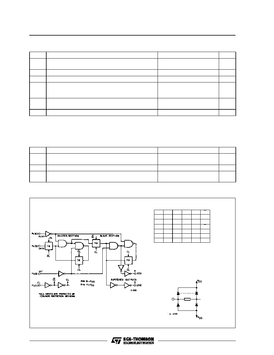
LOGIC DIAGRAM AND TRUTH TABLE (one of two identical flip≠flops)
NO CHANGE
LOGIC 0 = LOW
= LOW LEVEL
LOGIC 1 = HIGH
X = DON'T CARE
N(N) = FF1/FF2 TERMINAL
ASSIGNEMENT
CL
D
R
S
Q
Q
≠
/
≠
0
0
0
0
1
≠
/
≠
1
0
0
1
0
≠\
≠
X
0
0
Q
Q
X
X
1
0
0
1
X
X
0
1
1
0
X
X
1
1
1
1
HCC/HFC4013B
2/11
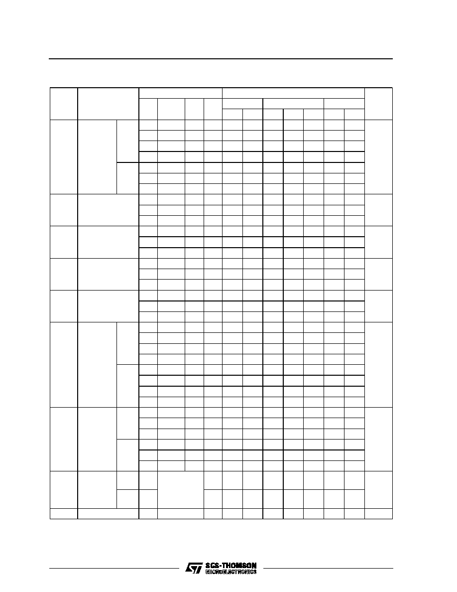
STATIC ELECTRICAL CHARACTERISTICS (over recommended operating conditions)
Test Conditions
Value
V
I
V
O
|I
O
|
V
D D
T
L o w
*
25
∞
C
T
Hig h
*
Symbol
Parameter
(V)
(V)
(
µ
A)
(V)
Min. Max. Min. Typ. Max. Min. Max.
Unit
I
L
Quiescent
Current
HCC
Types
0/5
5
1
0.02
1
30
µ
A
0/10
10
2
0.02
2
60
0/15
15
4
0.02
4
120
0/20
20
20
0.04
20
600
HCF
Types
0/5
5
4
0.02
4
30
0/10
10
8
0.02
8
60
0/15
15
16
0.02
16
120
V
O H
Output High
Voltage
0/5
< 1
5
4.95
4.95
4.95
V
0/10
< 1
10
9.95
9.95
9.95
0/15
< 1
15
14.95
14.95
14.95
V
O L
Output Low
Voltage
5/0
< 1
5
0.05
0.05
0.05
V
10/0
< 1
10
0.05
0.05
0.05
15/0
< 1
15
0.05
0.05
0.05
V
IH
Input High
Voltage
0.5/4.5
< 1
5
3.5
3.5
3.5
V
1/9
< 1
10
7
7
7
1.5/13.5
< 1
15
11
11
11
V
IL
Input Low
Voltage
4.5/0.5
< 1
5
1.5
1.5
1.5
V
9/1
< 1
10
3
3
3
13.5/1.5
< 1
15
4
4
4
I
O H
Output
Drive
Current
HCC
Types
0/5
2.5
5
≠ 2
≠ 1.6 ≠ 3.2
≠ 1.15
mA
0/5
4.6
5
≠ 0.64
≠ 0.51 ≠ 1
≠ 0.36
0/10
9.5
10
≠ 1.6
≠ 1.3 ≠ 2.6
≠ 0.9
0/15
13.5
15
≠ 4.2
≠ 3.4 ≠ 6.8
≠ 2.4
HCF
Types
0/ 5
2.5
5
≠ 1.53
≠ 1.36 ≠ 3.2
≠ 1.1
0/ 5
4.6
5
≠ 0.52
≠ 0.44 ≠ 1
≠ 0.36
0/10
9.5
10
≠ 1.3
≠ 1.1 ≠ 2.6
≠ 0.9
0/15
13.5
15
≠ 3.6
≠ 3.0 ≠ 6.8
≠ 2.4
I
O L
Output
Sink
Current
HCC
Types
0/5
0.4
5
0.64
0.51
1
0.36
mA
0/10
0.5
10
1.6
1.3
2.6
0.9
0/15
1.5
15
4.2
3.4
6.8
2.4
HCF
Types
0/5
0.4
5
0.52
0.44
1
0.36
0/10
0.5
10
1.3
1.1
2.6
0.9
0/15
1.5
15
3.6
3.0
6.8
2.4
I
IH
, I
IL
Input
Leakage
Current
HCC
Types
0/18
Any Input
18
±
0.1
±
10
≠ 5
±
0.1
±
1
µ
A
HCF
Types
0/15
15
±
0.3
±
10
≠5
±
0.3
±
1
C
I
Input Capacitance
Any Input
5
7.5
pF
* T
Low
= ≠ 55
∞
C for HCC device : ≠ 40
∞
C for HCF device.
* T
High
= + 125
∞
C for HCC device : + 85
∞
C for HCF device.
The Noise Margin for both "1" and "0" level is : 1V min. with V
DD
= 5V, 2V min. with V
DD
= 10V, 2.5 V min. with V
DD
= 15V.
HCC/HCF4013B
3/11
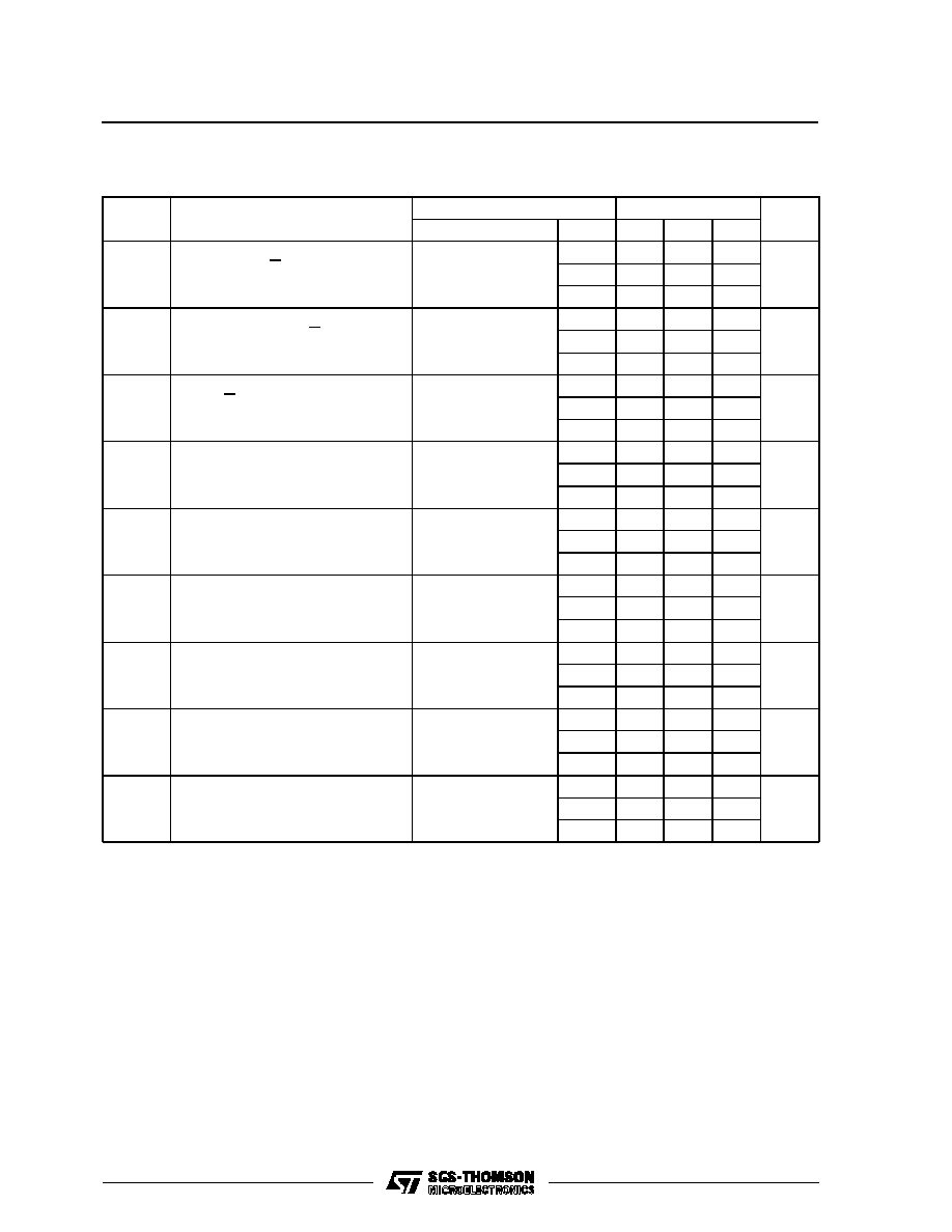
DYNAMIC ELECTRICAL CHARACTERISTICS (T
amb
= 25
∞
C, C
L
= 50pF, R
L
= 200k
,
typical temperature coefficient for all V
DD
= 0.3%/
∞
C values, all input rise and fall time = 20ns)
Val ue
Symbol
Parameter
Test Conditions
V
D D
(V)
Min.
Typ.
Max.
Unit
t
P L H
, t
P HL
Propagation Delay Time
(clock to Q or Q outputs)
5
150
300
ns
10
65
130
15
45
90
t
P L H
Propagation Delay Time
(set to Q or reset to Q)
5
150
300
ns
10
65
130
15
45
90
t
P HL
Propagation Delay Time
(set to Q or reset to Q)
5
200
400
ns
10
85
170
15
60
120
t
THL
, t
T L H
Transition Time
5
100
200
ns
10
50
100
15
40
80
f
CL
*
Maximum Clock Input Frequency
5
3.5
7
MHz
10
8
16
15
12
24
t
W
Cock Pulse Width
5
140
70
ns
10
60
30
15
40
20
t
r
, t
f
**
Clock Input Rise or Fall Time
5
15
µ
s
10
4
15
1
t
W
Set or Reset Pulse Width
5
180
90
ns
10
80
40
15
50
25
t
se t u p
Data Setup Time
5
40
20
ns
10
20
10
15
15
7
*
Input t
r
, t
f
= 5ns.
**
If more than unit is cascaded in a parallel clocked application, t
r
should be made less than or equal to the sum of the fixed
propagation delay time at 15pF and the transition time of the carry output driving stage for the estimated capacitive load.
HCC/HFC4013B
4/11
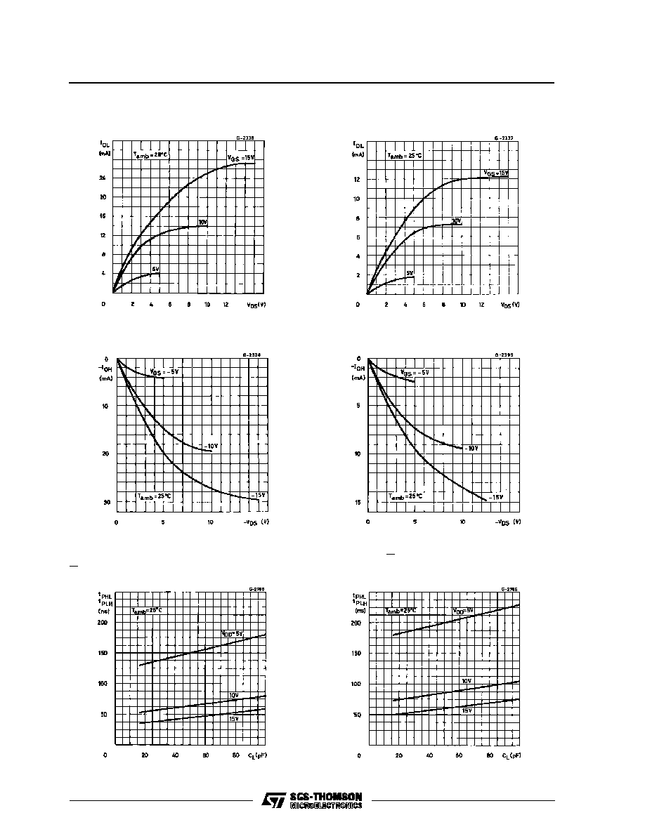
Typical Output Low (sink) Current Characteristics.
Minimum Output Low (sink) Current Charac-
teristics.
Typical Output High (source) Current Charac-
teristics.
Minimum Output High (source) Current Charac-
teristics.
Typical Propagation Delay Time vs. Load Capacit-
ance (SET to Q or RESET to Q).
Typical Propagation Delay Time vs. Load Capacit-
ance (CLOCK or SET to Q, CLOCK or RESET to
Q).
HCC/HCF4013B
5/11